Description
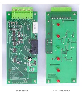
A printed circuit board (PCB) is a laminated sandwich structure of conductive and insulating layers. PCBs have two complementary functions. The first is to affix electronic components in designated locations on the outer layers by means of soldering. The second is to provide reliable electrical connections (and also reliable open circuits) between the component’s terminals in a controlled manner often referred to as PCB design. Each of the conductive layers is designed with an artwork pattern of conductors (similar to wires on a flat surface) that provides electrical connections on that conductive layer, while another manufacturing process adds vias – small and precisely located holes that are drilled through the laminate and then plated with copper. The vias are the electrical interconnection between layers that are otherwise insulated in the laminate structure and this allows a third dimension of connection between conductive layers in a controlled manner that is both reliable and cost-effective for mass production of electronic products.


Reviews
There are no reviews yet.